


As semiconductor devices, electronic components, and precision manufacturing systems continue to evolve toward higher integration and smaller form factors, traditional manufacturing methods face increasing challenges in producing complex structures with high accuracy, rapid iteration, and functional material compatibility.
In semiconductor and electronics industries, electrostatic discharge (ESD) protection is a critical requirement. Even a small amount of uncontrolled static electricity can damage sensitive electronic components, reduce product reliability, or impact manufacturing yield. Therefore, materials with controlled electrical conductivity and antistatic properties are increasingly required for manufacturing fixtures, tooling, packaging structures, and functional prototypes.
However, conventional machining and molding processes often struggle with low-volume production, complex geometries, and rapid customization. High-precision additive manufacturing provides a new approach by enabling engineers to directly fabricate intricate ESD-functional components with excellent design flexibility.
Powered by Projection Micro Stereolithography (PµSL) technology, BMF's microArch® S150 provides a powerful solution for producing precision ESD components with 25μm optical resolution, enabling semiconductor and electronics manufacturers to accelerate innovation and improve manufacturing efficiency.
Why ESD Materials Matter in Semiconductor and Electronics Manufacturing
Electronic devices are becoming increasingly sensitive due to advanced semiconductor processes, miniaturized circuits, and high-density packaging technologies. During manufacturing, transportation, and testing processes, electrostatic discharge can damage electronic components, reduce their performance, shorten the service life of components, and pose safety hazards.
To prevent these risks, ESD materials are widely used in semiconductor handling tools, electronic component trays, precision assembly tooling, protective housings and custom structures,etc. High-resolution 3D printing with ESD materials provides an alternative manufacturing pathway, allowing engineers to create customized components without expensive tooling or long production cycles.
microArch® S150: 25μm Optical Resolution for Functional ESD Components
The microArch® S150 is a desktop micro-precision 3D printing system developed for advanced prototyping and manufacturing applications. Based on BMF's PµSL technology, the system delivers 25μm optical resolution, enabling the fabrication of detailed structures with excellent surface quality and dimensional consistency.
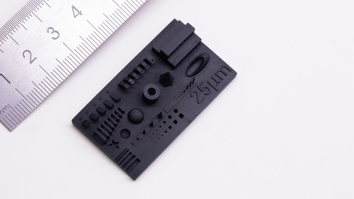
S150 Standard Demo Part
Key advantages of microArch® S150 for ESD applications
1. High Resolution for Complex Electronic Structures
With 25μm optical resolution, the S150 can produce intricate geometries required for advanced electronic applications. The ability to directly manufacture detailed structures enables engineers to move beyond traditional machining limitations and explore new designs optimized for modern electronics.
2. Functional Material Compatibility for ESD Applications
For semiconductor and electronic manufacturing environments, mechanical performance alone is not sufficient. Functional material properties, such as electrostatic control, are essential. Combined with S150's precision printing capability, ESD materials expand the application possibilities of polymer additive manufacturing from simple prototypes to functional engineering components.
3. Rapid Prototyping for Semiconductor Equipment Development
The semiconductor industry requires continuous innovation in packaging, testing, and manufacturing processes. Engineers frequently need customized tools and fixtures designed for specific components or production scenarios.

The samples from left to right are as follows:Chip Socket,Circular Connector,CPU Socket
With microArch® S150, engineers can directly print functional ESD components from digital designs, significantly shortening development cycles. This rapid iteration capability enables faster validation of new concepts and reduces development costs.
From Prototype to Production: A More Flexible Manufacturing Approach
The integration of ESD materials with high-precision 3D printing represents a shift from traditional manufacturing toward more agile production methods. For semiconductor and electronics companies, this approach offers faster product development cycles and greater design freedom.
The microArch® S150 provides an accessible platform for laboratories, engineering teams, and manufacturers seeking to explore advanced micro-scale additive manufacturing. With its compact desktop design, 25μm optical resolution, and compatibility with functional materials, S150 helps bridge the gap between research innovation and industrial application.
As semiconductor devices and electronic systems become increasingly sophisticated, manufacturers need production technologies that combine precision, flexibility, and functional performance. BMF's micro-precision 3D printing technology provides a powerful solution for the next generation of semiconductor and electronics innovation, helping companies accelerate development, optimize manufacturing processes, and transform complex designs into reality.